|
|
|
|
 |
 |
|
|
|
|
|
|
|
|
|
|
|
|
|
|
|
|
|
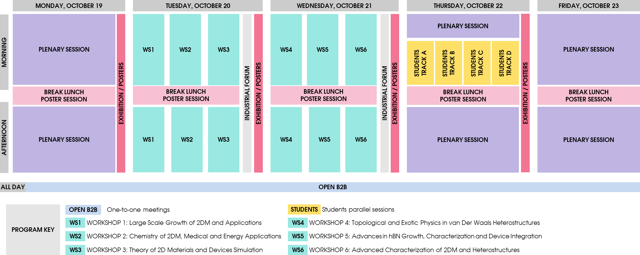
Tue 20 |
|
Wed 21 |
|
Thu 22 |
|
Fri 23 |
|
|
|
|
|
|
|
|
|
|
|
|
|
|
|
|
|
|
|
|
|
|
|
|
|
|
|
|
|
|
|
|
|
|
|
|
|
|
|
|
|
|
|
|
|
|
|
|
|
|
|
|
|
|
|
|
|
|
|
|
|
|
|
|
09:00-09:30 |
|
INVITED |
|
Quantum interferences and spin orbit interactions in Graphene/TMD heterostructures
|
|
Helene Bouchiat,
Universite Paris SUD / CNRS, France |
|
 |
|
|
|
|
|
|
|
|
|
|
|
|
|
|
|
|
|
|
09:30-10:00 |
|
INVITED |
|
Controlling Spin-Orbit Torques Through Symmetry
using Van der Waals Materials
|
|
Marcos H. Diniz Guimaraes,
University of Groningen, The Netherlands |
|
|
|
|
|
|
|
|
|
|
|
|
|
|
|
|
|
|
|
|
10:00-10:15 |
|
|
Unusual Spin-Orbit Torque in Magnetic Janus Transition Metal Dichalcogenides |
|
Jose H. Garcia Aguilar,
Catalan Institute of Nanoscience and Nanotechnology, Spain |
|
|
|
|
|
|
|
|
|
|
|
|
|
|
|
|
|
|
|
|
10:15-10:30 |
|
|
Large multi-directional spin-to-charge conversion in low symmetry semimetal MoTe2 at room temperature |
|
Nerea Ontoso,
CIC nanoGUNE BRTA, Spain |
|
|
|
|
|
|
|
|
|
|
|
|
|
|
|
|
|
|
|
|
10:30-13:00 |
|
Break / ePoster Session / Exhibition |
|
|
|
|
|
|
|
|
|
|
|
|
|
|
|
|
|
|
|
|
|
|
|
|
|
|
|
|
|
|
|
|
|
|
14:00-14:30 |
|
INVITED |
|
Quantum Manipulation of Molecular Graphene
|
|
Lapo Bogani,
University of Oxford, UK |
|
|
|
|
|
|
|
|
|
|
|
|
|
|
|
|
|
|
|
|
14:30-15:00 |
|
INVITED |
|
Light-induced anomalous Hall effect in graphene
|
|
James McIver,
Max Planck Institute for the Structure and Dynamics of Matter, CFEL, Germany |
|
|
|
|
|
|
|
|
|
|
|
|
|
|
|
|
|
|
|
|
15:00-15:15 |
|
|
Experimental detection of graphene’s singular orbital diamagnetism at the Dirac point. |
|
Jorge Vallejo Bustamante,
Laboratoire de Physique des Solides, France |
|
|
|
|
|
|
|
|
|
|
|
|
|
|
|
|
|
|
|
|
15:15-15:30 |
|
|
Transport experiments in twisted (double) bilayer graphene |
|
Peter Rickhaus,
ETH Zürich, Switzerland |
|
|
|
|
|
|
|
|
|
|
|
|
|
|
|
|
|
|
|
|
15:30-16:30 |
|
Break / ePoster Session / Exhibition |
|
|
|
|
|
|
|
|
|
|
|
|
|
|
|
|
|
|
16:30-17:00 |
|
INVITED |
|
Helical quantum Hall phase in graphene on SrTiO3
|
|
Benjamin Sacépé,
Institut Néel - CNRS, France |
|
|
|
|
|
|
|
|
|
|
|
|
|
|
|
|
|
|
|
|
17:00-17:15 |
|
|
Multi-frequency Shubnikov-de Haas oscillations in topological semimetal Pt2HgSe3 |
|
Diego Mauro,
University of Geneva, Switzerland |
|
|
|
|
|
|
|
|
|
|
|
|
|
|
|
|
|
|
|
|
17:15-17:45 |
|
INVITED |
|
Controlling magnetism and exchange interaction mechanisms in van der Waals ferromagnet Cr2Ge2Te6
|
|
Hidekazu Kurebayashi,
UCL, UK |
|
|
|
|
|
|
|
|
|
|
|
|
|
|
|
|
|
|
|
|
|
|
|
|
|
|
|
|
|
|
|
|
|
|
|
|
|
09:00-09:15 |
|
Introduction: Annick Loiseau |
|
|
|
|
|
|
|
|
|
|
|
|
|
|
|
|
|
|
09:15-09:45 |
|
INVITED |
|
Stacking and twisting 2D materials for quantum nano-optoelectronics
|
|
Frank Koppens,
ICREA/ICFO, Spain |
|
|
|
|
|
|
|
|
|
|
|
|
|
|
|
|
|
|
|
|
09:45-10:15 |
|
INVITED |
|
Graphene Photonics for High Data Rate Modulators and Detectors
|
|
Marco Romagnoli,
CNIT, Italy |
|
|
|
|
|
|
|
|
|
|
|
|
|
|
|
|
|
|
|
|
10:15-10:45 |
|
INVITED |
|
2D Materials for MTJs: from band spin filtering to hybridization/spinterface
|
|
Pierre Seneor,
Université Paris-Sud / CNRS, France |
|
|
|
|
|
|
|
|
|
|
|
|
|
|
|
|
|
|
|
|
10:45-11:30 |
|
Break / ePoster Session / Exhibition |
|
|
|
|
|
|
|
|
|
|
|
|
|
|
|
|
|
|
11:30-12:00 |
|
INVITED |
|
Platforms to develop 2D materials integrated with Si
|
|
Cedric Huyghebaert,
IMEC, Belgium |
|
|
|
|
|
|
|
|
|
|
|
|
|
|
|
|
|
|
|
|
12:00-12:15 |
|
|
Excellent Electronic Transport in Heterostructures of Graphene and Monoisotopic Boron-Nitride Grown at Atmospheric Pressure |
|
Jens Sonntag,
RWTH Aachen, Germany |
|
|
|
|
|
|
|
|
|
|
|
|
|
|
|
|
|
|
|
|
12:15-13:00 |
|
Panel discussion: h-BN requirements - Koppens/Romagnoli/Seneor/Cedric/Sonntag |
|
|
|
|
|
|
|
|
|
|
|
|
|
|
|
|
|
|
|
|
|
|
|
|
|
|
|
|
|
|
|
|
|
|
14:00-14:30 |
|
INVITED |
|
Highly Controlled CVD Synthesis of Monolayer and Multilayer h-BN for 2D Materials Applications
|
|
Hiroki Ago,
Kyushu University, Japan |
|
|
|
|
|
|
|
|
|
|
|
|
|
|
|
|
|
|
|
|
14:30-15:00 |
|
INVITED |
|
Original ways to large h-BN single crystals and derived nanosheets
|
|
Bérangère Toury,
Université de Lyon, France |
|
|
|
|
|
|
|
|
|
|
|
|
|
|
|
|
|
|
|
|
15:00-15:30 |
|
INVITED |
|
On the Fundamental Mechanisms that underpin CVD Technology for Atomically Thin 2D Films
|
|
Stephan Hofmann,
University of Cambridge, UK |
|
|
|
|
|
|
|
|
|
|
|
|
|
|
|
|
|
|
|
|
15:30-15:45 |
|
|
High mobility scalable graphene/h-BN heterostructures |
|
Leonardo Martini,
Istituto Italiano di Tecnologia, Italy |
|
|
|
|
|
|
|
|
|
|
|
|
|
|
|
|
|
|
|
|
15:45-16:00 |
|
|
Molecular beam epitaxial growth of hexagonal boron nitride on Ni |
|
Jawad Hadid,
IEMN-CNRS, France |
|
|
|
|
|
|
|
|
|
|
|
|
|
|
|
|
|
|
|
|
16:00-16:30 |
|
Break / ePoster Session / Exhibition |
|
|
|
|
|
|
|
|
|
|
|
|
|
|
|
|
|
|
16:30-17:00 |
|
INVITED |
|
Solution Growth and Properties of Monoisotopic Hexagonal Boron Nitride Single Crystals
|
|
James H. Edgar,
Kansas State University, USA |
|
|
|
|
|
|
|
|
|
|
|
|
|
|
|
|
|
|
|
|
17:00-17:30 |
|
INVITED |
|
Towards synthesis and characterization of large scale BN films
|
|
Annick Loiseau,
ONERA, France |
|
|
|
|
|
|
|
|
|
|
|
|
|
|
|
|
|
|
|
|
17:30-18:00 |
|
INVITED |
|
BN materials for 2D devices : learnings from optical properties
|
|
Julien Barjon,
Université de Versailles St-Quentin-En-Yvelines, France |
|
|
|
|
|
|
|
|
|
|
|
|
|
|
|
|
|
|
|
|
18:00-18:30 |
|
Panel Discussion: Growth/characterization/transfer: How do we grow large area h-BN single crystal growth |
|
|
|
|
|
|
|
|
|
|
|
|
|
|
|
|
|
|
|
|
|
|
|
|
|
|
|
|
|
|
|
|
|
|
|
09:00-09:30 |
|
INVITED |
|
Photoemission electron spectromicroscopy of complex interfaces: probing 2D materials and the support underneath
|
|
Andrea Locatelli,
Elettra-Sincrotrone Trieste, Italy |
|
|
|
|
|
|
|
|
|
|
|
|
|
|
|
|
|
|
|
|
09:30-09:45 |
|
|
Investigating electronics of 2D materials and heterostructures by photoemission electron microscopy |
|
Olivier Renault,
CEA-LETI, France |
|
|
|
|
|
|
|
|
|
|
|
|
|
|
|
|
|
|
|
|
09:45-10:15 |
|
INVITED |
|
An atomic-scale look at point defects in truly 2D semiconductors
|
|
Sara Barja,
UPV/EHU, Spain |
|
|
|
|
|
|
|
|
|
|
|
|
|
|
|
|
|
|
|
|
10:15-10:30 |
|
|
Filtering the Photoluminescence of atomically-thin semiconductors with Graphene |
|
Luis Enrique Parra Lopez,
Strasbourg University, France |
|
|
|
|
|
|
|
|
|
|
|
|
|
|
|
|
|
|
|
|
10:30-13:00 |
|
Break / ePoster Session / Exhibition |
|
|
|
|
|
|
|
|
|
|
|
|
|
|
|
|
|
|
|
|
|
|
|
|
|
|
|
|
|
|
|
|
|
|
14:00-14:30 |
|
INVITED |
|
Measuring graphene’s Berry phase at B = 0 T
|
|
Vincent Renard,
Université Grenoble Alpes / CEA, France |
|
|
|
|
|
|
|
|
|
|
|
|
|
|
|
|
|
|
|
|
14:30-15:00 |
|
INVITED |
|
Measuring the local thermoelectric properties of graphene
|
|
Pascal Gehring,
UClouvain, Belgium |
|
|
|
|
|
|
|
|
|
|
|
|
|
|
|
|
|
|
|
|
15:00-15:15 |
|
|
Ghost Anti-Crossing caused by Umklapp Scattering in 2D Heterostructures |
|
Matthew Hamer,
The University of Manchester , UK |
|
|
|
|
|
|
|
|
|
|
|
|
|
|
|
|
|
|
|
|
15:15-15:30 |
|
|
Electronic coupling in the F4-TCNQ/single-layer GaSe heterostructure |
|
Lama Khalil,
C2N, France |
|
|
|
|
|
|
|
|
|
|
|
|
|
|
|
|
|
|
|
|
15:30-15:45 |
|
|
Spin-Orbit Coupling in Graphene-MoS2 Hybrid Structures: an X-Ray Absorption Spectroscopy Study |
|
Adriana Figueroa,
Catalan Institute of Nanoscience and Nanotechnology (ICN2), Spain |
|
|
|
|
|
|
|
|
|
|
|
|
|
|
|
|
|
|
|
|
15:45-16:00 |
|
|
Effect of nitrogen doping of graphene on the electronic interaction with organic molecules |
|
Jérôme Lagoute,
Université de Paris, CNRS, France |
|
|
|
|
|
|
|
|
|
|
|
|
|
|
|
|
|
|
|
|
16:00-16:30 |
|
Break / ePoster Session / Exhibition |
|
|
|
|
|
|
|
|
|
|
|
|
|
|
|
|
|
|
16:30-17:00 |
|
INVITED |
|
To be defined
|
|
Jamie Warner,
University of Oxford, UK |
|
|
|
|
|
|
|
|
|
|
|
|
|
|
|
|
|
|
|
|
17:00-17:15 |
|
|
High-quality N doped graphene layers: "inside out" growth and reactivity |
|
Mirco Panighel,
CNR-IOM, Italy |
|
|
|
|
|
|
|
|
|
|
|
|
|
|
|
|
|
|
|
|
17:15-17:30 |
|
|
Study of the van der Waals epitaxy of WSe2 on mica |
|
Alain Marty,
IRIG/Spintec-CEA, France |
|
|
|
|
|
|
|
|
|
|
|
|
|
|
|
|
|
|
|
|
17:30-17:45 |
|
|
Narrow Energy Distributions of Electrons Emitted From Clean Graphene Field Emission of Clean Graphene |
|
Philippe Poncharal,
University of Lyon, France |
|
|
|
|
|
|
|
|
|
|
|
|
|
|
|
|
|
|
|
|
|
|
|
|
|
|
|
|
|
|
|
|
|
|
|
|
|
09:00-09:30 |
|
KEYNOTE |
|
Targeting the Mass Production of CVD Graphene |
|
Zhongfan Liu,
Peking University, China |
|
|
|
|
|
|
|
|
|
|
|
|
|
|
|
|
|
|
|
|
09:30-09:45 |
|
INVITED |
|
Dry transfer key to scalable production and integration of graphene
|
|
Richard Van Rijn,
Applied Nanolayers B.V., The Netherlands |
|
|
|
|
|
|
|
|
|
|
|
|
|
|
|
|
|
|
|
|
09:45-10:00 |
|
INVITED |
|
Scaling up Production of Graphene Oxide
|
|
Samaneh Etemadi,
Abalonyx, Norway |
|
|
|
|
|
|
|
|
|
|
|
|
|
|
|
|
|
|
|
|
10:00-10:15 |
|
INVITED |
|
From labs to pilot lines: Graphene and related materials device fabrication solutions
|
|
Ravi Sundaram,
Oxford Instruments, UK |
|
|
|
|
|
|
|
|
|
|
|
|
|
|
|
|
|
|
|
|
10:15-10:30 |
|
INVITED |
|
In-situ functionalized E-Graphenes and the potential for energy storage and hydrogen production
|
|
Martin R. Lohe,
Sixonia Tech GmbH, Germany |
|
|
|
|
|
|
|
|
|
|
|
|
|
|
|
|
|
|
|
|
10:30-10:40 |
|
|
Wafer Scale Integration of Graphene – Progress and Outlook |
|
Zhenxing Wang,
AMO GmbH, Germany |
|
|
|
|
|
|
|
|
|
|
|
|
|
|
|
|
|
|
|
|
10:40-10:50 |
|
|
Towards transfer-free large area fabrication of gas filtration devices based on a suspended porous graphene mono-layer. |
|
Hélène Le Poche,
CEA LITEN/DTNM, France |
|
|
|
|
|
|
|
|
|
|
|
|
|
|
|
|
|
|
|
|
10:50-11:30 |
|
Break / ePoster Session / Exhibition |
|
|
|
|
|
|
|
|
|
|
|
|
|
|
|
|
|
|
11:30-11:45 |
|
INVITED |
|
Sensing and biosensing using graphene-based materials
|
|
Arben Merkoci,
ICREA-ICN2, Spain |
|
|
|
|
|
|
|
|
|
|
|
|
|
|
|
|
|
|
|
|
11:45-12:00 |
|
INVITED |
|
Graphene Electro-mechanical Bio-sensors
|
|
Aravind Vijayaraghavan,
The University of Manchester, UK |
|
|
|
|
|
|
|
|
|
|
|
|
|
|
|
|
|
|
|
|
12:00-12:10 |
|
|
Graphene, the ideal neural interface candidate |
|
Carolina Aguilar,
INBRAIN, Spain |
|
|
|
|
|
|
|
|
|
|
|
|
|
|
|
|
|
|
|
|
12:10-12:20 |
|
|
Enabling a world of enhanced vision |
|
Stijn Goossens,
QURV, Spain |
|
|
|
|
|
|
|
|
|
|
|
|
|
|
|
|
|
|
|
|
12:20-12:30 |
|
|
2D light emitting devices for silicon photonics |
|
Yue Wang,
University of York, UK |
|
|
|
|
|
|
|
|
|
|
|
|
|
|
|
|
|
|
|
|
12:30-12:40 |
|
|
120Gb/s ultra-fast photo-thermo-electric graphene photodetector for optical communications |
|
Simone Marconi,
Sant´Anna School of Advanced Studies, Italy |
|
|
|
|
|
|
|
|
|
|
|
|
|
|
|
|
|
|
|
|
12:40-12:50 |
|
|
Development of Amplifier integrated circuits based on graphene field effect transistors |
|
Wei Wei,
University of Lille - IEMN, France |
|
|
|
|
|
|
|
|
|
|
|
|
|
|
|
|
|
|
|
|
|
|
|
|
|
|
|
|
|
|
|
|
|
|
|
|
14:15-14:30 |
|
INVITED |
|
GRAPHENE PRODUCTION - Graphene is already on several markets
|
|
Honoré Tsotetzo,
Graphene Production, France |
|
|
|
|
|
|
|
|
|
|
|
|
|
|
|
|
|
|
|
|
14:30-14:40 |
|
|
Low-voltage 2D materials-based printed field-effect transistors on paper |
|
Silvia Conti,
University of Pisa, Italy |
|
|
|
|
|
|
|
|
|
|
|
|
|
|
|
|
|
|
|
|
14:40-14:50 |
|
|
Graphene nanosheets produced by a green liquid phase exfoliation process |
|
Svetlana Ponomareva,
University of Alpes Grenoble, France |
|
|
|
|
|
|
|
|
|
|
|
|
|
|
|
|
|
|
|
|
14:50-15:00 |
|
|
The role of graphene in membrane distillation technology towards portable desalination devices |
|
Matilde Eredia,
BeDimensional S.p.a, Italy |
|
|
|
|
|
|
|
|
|
|
|
|
|
|
|
|
|
|
|
|
15:00-15:10 |
|
|
Metallic 2D crystals for bifunctional, pH-universal electrocatalysts for water splitting reactions |
|
Sebastiano Bellani,
Bedimensional Spa, Italy |
|
|
|
|
|
|
|
|
|
|
|
|
|
|
|
|
|
|
|
|
15:10-15:20 |
|
|
Graphene-Enabled Electrically-Controlled Functional Textiles |
|
M. Said Ergoktas,
The University of Manchester, UK |
|
|
|
|
|
|
|
|
|
|
|
|
|
|
|
|
|
|
|
|
15:20-16:00 |
|
Break / ePoster Session / Exhibition |
|
|
|
|
|
|
|
|
|
|
|
|
|
|
|
|
|
|
16:00-16:15 |
|
INVITED |
|
Direct Correlative Nanoscopy Imaging of 2D Materials
|
|
Marc Chaigneau,
HORIBA FRANCE SAS, France |
|
|
|
|
|
|
|
|
|
|
|
|
|
|
|
|
|
|
|
|
16:15-16:25 |
|
|
Nanoscale Optical Imaging of Graphene using s-SNOM |
|
Philip Schaefer,
neaspec GmbH, Germany |
|
|
|
|
|
|
|
|
|
|
|
|
|
|
|
|
|
|
|
|
16:25-16:35 |
|
|
SAMSON – Integrated Software Platform for Molecular Design |
|
Stephane Redon,
OneAngstrom, France |
|
|
|
|
|
|
|
|
|
|
|
|
|
|
|
|
|
|
|
|
16:35-16:45 |
|
|
NanoFrazor – A Nanolithography Tool for 2D & 3D Devices |
|
Nils Goedecke,
Heidelberg Instruments Nano, Switzerland |
|
|
|
|
|
|
|
|
|
|
|
|
|
|
|
|
|
|
|
|
16:45-16:55 |
|
|
Nano-electrical characterization of 2D materials with Atomic Force Microscope |
|
Paco Martinez,
CSInstruments, Spain |
|
|
|
|
|
|
|
|
|
|
|
|
|
|
|
|
|
|
|
. |
|
|
|
|
|
|
|
|
|
|
|
|
|
|
|
|
|
|
|
|
|
 |
|
 Workshop 1: Large scale growth of 2DM and applications Workshop 1: Large scale growth of 2DM and applications
The workshop targets to overview most promising advances in two-dimensional material growth (graphene and transition metal dichalcogenides) in the context of high-technologies such as photonics and plasmonics, sensing, electronics or medical devices. Focus on experimental equipment, scalability and challenges in producing defect-free materials will be addressed, as well as their co-integration in functional devices, including field effect transistors, optical switches, photodetectors.
|
| |
| | |
 |
|
Peter Bøggild |
DTU Physics |
Denmark |
Invited |
|
|
|
 |
|
Alex Jouvray |
Aixtron |
UK |
Invited |
|
|
|
 |
|
Satender Kataria |
RWTH Aachen University |
Germany |
Invited |
|
|
 |
|
Cecilia Mattevi |
Imperial College London |
UK |
Invited |
|
|
|
 |
|
Joshua A. Robinson |
Pennsylvania State University |
USA |
Invited |
|
|
|
|
| |
|
| |
Workshop 2: Chemistry of 2DM, Medical and Energy Applications
This workshop will focus on the progress of the chemical approaches towards graphene and related 2D materials. Top-down chemical exfoliation and bottom-up growth and synthesis of GRMs, as well as the chemical functionalization of GRMs with covalent and non-covalent approaches leading to tunable properties will be presented. Other topics including hierarchical hybrid structures, polymer composites, solution processing, electrocatalysis & photocatalysis, functional foams, membranes and coatings of GRMs will be also presented.
|
| |
| | |
 |
|
Sang Ouk Kim |
KAIST |
South Korea |
Invited |
|
|
|
 |
|
Paolo Samorì |
Université de Strasbourg |
France |
Invited |
|
|
|
 |
|
Andrey Turchanin |
Friedrich Schiller University Jena |
Germany |
Invited |
|
|
|
|
|
|
|
|
|
| |
|
| |
| Workshop 3: Theory of 2D Materials and Devices Simulation
This workshop aims at presenting recent theoretical advances and simulation studies of optical, magnetic and spin transport phenomena in graphene, two-dimensional materials (2DM), as well as more complex vdW heterostructures. Emphasis will be given to concepts such as valleytronics, dynamics of excitons, as well as the emerging field of twistronics. A particular focus will be also given to the physics emerging from 2D magnetic materials and their interfacing with other 2DM such as TMD and others to trigger spintronic applications. |
| |
| | |
 |
|
Mark-Oliver Goerbig |
CNRS, Université Paris-Sud |
France |
Invited |
|
|
|
 |
|
Mikito Koshino |
Osaka University |
Japan |
Invited |
|
|
|
 |
|
Yazyev Oleg |
EPLF |
Switzerland |
Invited |
|
|
|
|
|
|
|
|
| |
|
| |
| Workshop 4: Topological and Exotic Physics in van Der Waals Heterostructures
This workshop will address the recent progress and current challenges in assembling two-dimensional materials to generate new physical properties such as exotic superconductivity, Mott insulating phases, Ferromagnetism and so on in few layers’ systems, as well as the search of strategies for manipulating quantum degrees of freedom (spin, valley, sublattice pseudospin) and to trigger quantum topological phases (such as quantum spin hall effect, quantum anomalous Hall effect, spin and valley hall effects,…). |
| |
| | |
 |
|
Lapo Bogani |
University of Oxford |
UK |
Invited |
|
|
|
 |
|
Helene Bouchiat |
Universite Paris SUD / CNRS |
France |
Invited |
|
|
|
 |
|
Marcos H. Diniz Guimaraes |
University of Groningen |
The Netherlands |
Invited |
|
|
|
 |
|
Hidekazu Kurebayashi |
UCL |
UK |
Invited |
|
|
|
 |
|
James McIver |
Max Planck Institute for the Structure and Dynamics of Matter, CFEL |
Germany |
Invited |
|
|
|
 |
|
Benjamin Sacépé |
Institut Néel - CNRS |
France |
Invited |
|
|
|
| |
|
| |
Workshop 5: Advances in hBN growth, characterization and device integration
The workshop will focus on the recent progress concerning the experimental growth techniques developed to upscale the size of hexagonal Boron-Nitride (hBN) at monolayer or multilayer level. Advances and challenges in CVD growth, epitaxial or alternative techniques to produce high-quality large single crystals of hBN will be addressed as well as their characterization and integration into functional devices. The workshop will also cover various applications of this optical material such as deep UV emitters and detectors, single photon emitters from point defects, high room-temperature proton conductivity, field effect transistors (FETs), tunneling devices, photoelectric devices, and spin devices..
|
| |
| | |
 |
|
Hiroki Ago |
Kyushu University |
Japan |
Invited |
|
|
|
 |
|
Julien Barjon |
Université de Versailles St-Quentin-En-Yvelines |
France |
Invited |
|
|
|
 |
|
James H. Edgar |
Kansas State University |
USA |
Invited |
|
|
|
 |
|
Stephan Hofmann |
University of Cambridge |
UK |
Invited |
|
|
|
 |
|
Cedric Huyghebaert |
IMEC |
Belgium |
Invited |
|
|
|
 |
|
Frank Koppens |
ICREA/ICFO |
Spain |
Invited |
|
|
|
| | |
 |
|
Annick Loiseau |
ONERA |
France |
Invited |
|
|
|
 |
|
Marco Romagnoli |
CNIT |
Italy |
Invited |
|
|
|
 |
|
Pierre Seneor |
Université Paris-Sud / CNRS |
France |
Invited |
|
|
|
 |
|
Bérangère Toury |
Université de Lyon |
France |
Invited |
|
|
|
|
|
|
|
| |
|
| |
Workshop 6: Advanced Characterization of 2DM and heterostructures
The workshop focuses on recent advances and challenges in the characterization of 2D materials, van der Waals architectures and 2D material-based devices. Properties and phenomena investigated at the mesoscopic, nano and atomic scales using diverse advanced techniques will be covered, e.g. growth, defects, chemical functionalization, heterojunctions, charge transfer and dynamics, light emission, device operation. The scope will include a wide range of characterization methods that are critical for the study of 2D materials, such as microscopy, spectroscopy and transport / photo-transport measurements. The workshop will also address multimodal/multidimensional approaches that allow a simultaneous acquisition of several information channels (e.g. structural/chemical, structural/opto-electronic…), in-situ manipulations, time-resolved measurements and operando characterization. |
| |
| | |
 |
|
Sara Barja |
UPV/EHU |
Spain |
Invited |
|
|
|
 |
|
Pascal Gehring |
UClouvain |
Belgium |
Invited |
|
|
 |
|
Andrea Locatelli |
Elettra-Sincrotrone Trieste |
Italy |
Invited |
|
|
|
 |
|
Vincent Renard |
Université Grenoble Alpes / CEA |
France |
Invited |
|
|
|
 |
|
Jamie Warner |
University of Oxford |
UK |
Invited |
|
|
|
|
| |
|
| |
A series of targeted talks given by Invited speakers will be followed by oral contributions selected from the Graphene 2020 submissions on all workshops mentioned above. |
| |
| |
|
|
|
|
|
|